


The Application of SEM Scanning Electron Microscope in PCB Manufacturing and Failure Analysis
In the field of printed circuit board (PCB) manufacturing, as electronic products develop towards miniaturization and high density, the requirements for the reliability and precision of circuit boards are increasing day by day. Scanning electron microscopy (SEM), as a high-resolution microscopic analysis tool, has become an indispensable technical means in PCB quality control and failure analysis.
SEM is acronym of Scanning Electron Microscope。
A scanning electron microscope (SEM) is an electron optical instrument used to magnify and observe the surface structure of objects. It consists of a tube, an electronic signal collection and processing system, and an electronic signal display and recording system. The working principle of SEM is to observe and analyze the surface or fracture morphology of the sample through the interaction between electrons and substances. A finely focused electron beam is used to bombard the sample surface, generating signals such as secondary electrons and backscattered electrons.
Its high resolution (up to the nanometer level) and large depth of field make the microstructure in PCB manufacturing clearly visible, providing engineers with an intuitive basis for analyzing and improving the process.
01 Unveiling the Basic Principles of SEM
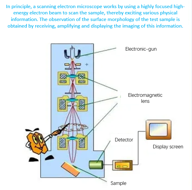
SEM uses a high-energy electron beam to scan the surface of a sample and acquires microscopic information about the sample surface by detecting various signals generated from the interaction between the electron beam and the sample.
Its working principle can be divided into three core steps: electron beam generation, signal excitation and signal collection imaging.
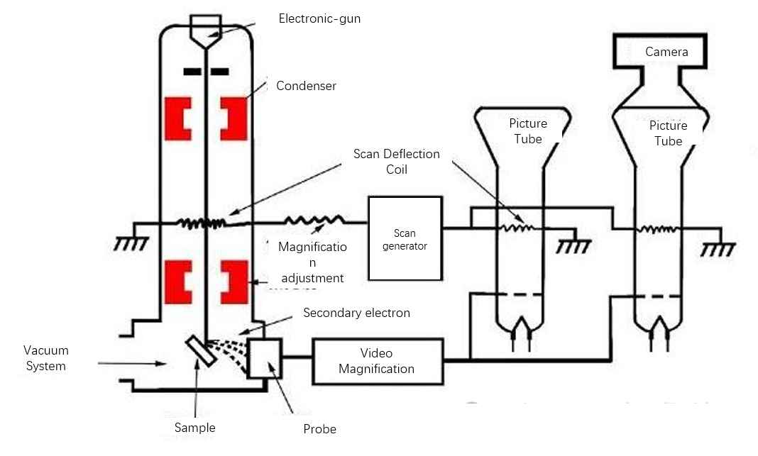
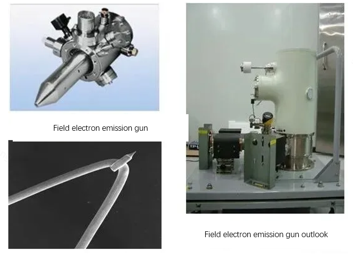
The electron gun emits electrons, which, under the acceleration of a high-voltage electric field (typically 0.3-30kV), are focused into extremely fine electron probes through an electromagnetic lens system.
The scanning coil controls the electron beam to perform a grating-like scan on the sample surface, exciting various physical signals such as secondary electrons and backscattered electrons.
The detector captures these signals, amplifies them and converts them into images reflecting the surface characteristics of the sample.
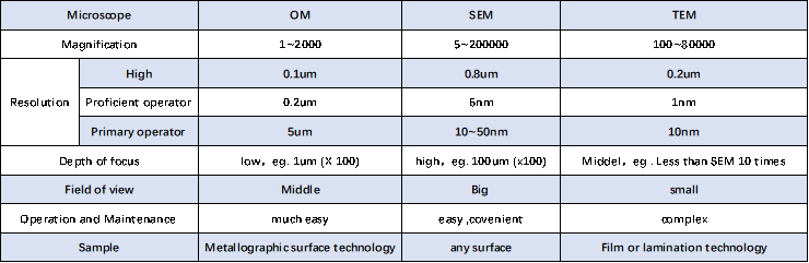
Compared with traditional optical microscopes, SEM has a higher magnification (usually up to 100,000 to 200,000 times) and a greater depth of field (about 300 times that of optical microscopes), and can present clear three-dimensional images. It is particularly suitable for observing the microstructure of rough surfaces.
![]()
02 The various signal types of scanning electron microscopes
The interaction between an electron beam and a solid sample generates various physical signals. Depending on the generation mechanism and application, they mainly include the following types:
Secondary electrons (SE) are electrons outside the nucleus of the sample that are bombarded by incident electrons and have relatively low energy (<50 eV)
Because it comes from the surface layer of the sample at 5-10nm, it is highly sensitive to the surface morphology and is the most important signal for observing the surface morphology of the sample.
Main application: Surface topography imaging. This is the most commonly used and fundamental function of SEM.
Backscattered electrons (BSE) are high-energy electrons that bounce back after incident electrons collide with atomic nuclei. Their yield increases with the increase of atomic serial number.
A depth range of several hundred nanometers from the surface of the sample can be used for component analysis and microstructure research.
Main uses: Component contrast imaging (atomic serial number contrast) and crystal orientation analysis.
Characteristic X-rays are electromagnetic wave radiation with characteristic energy released when electrons in the inner layers of an atom are excited and transition. They can be used for qualitative and quantitative analysis of elements and are usually used in conjunction with energy dispersive spectrometers (EDS). Main uses: Qualitative and quantitative analysis of elemental composition. It usually needs to be used in conjunction with an energy dispersive spectrometer (EDS/EDX).
Absorbed electrons are the electrons absorbed by the sample after the incident electrons have lost their energy. Their signal strength is complementary to that of backscattered electrons and secondary electrons.
Main application: Its signal strength is complementary to the backscattered electron signal and can also be used for component contrast imaging, but its application is less.
Auger electrons are low-energy electrons emitted from a very limited number of atomic layers (about 1nm) on the sample surface and are suitable for surface chemical composition analysis.
Transmitted electrons are electrons that penetrate thin samples and can be used to observe the internal structure of the samples.
Main application: Internal structure analysis under scanning transmission electron microscopy (STEM) mode.
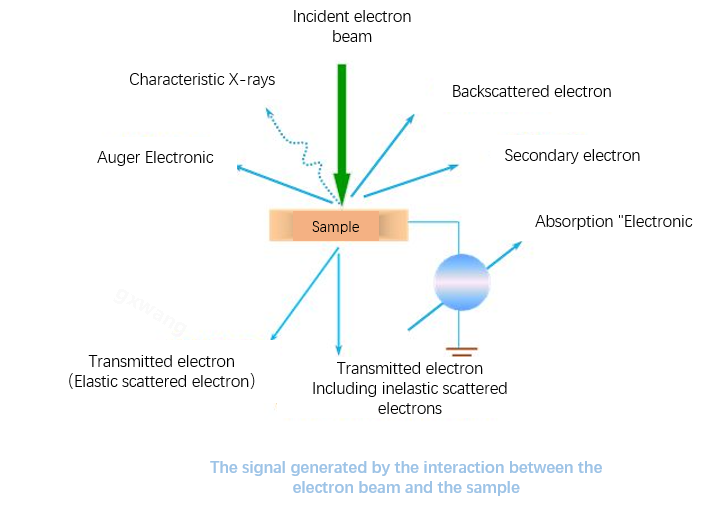
![]() For conventional PCB failure analysis, secondary electrons, backscattered electrons and characteristic X-rays (EDS) are the three most core and commonly used signals.
For conventional PCB failure analysis, secondary electrons, backscattered electrons and characteristic X-rays (EDS) are the three most core and commonly used signals.
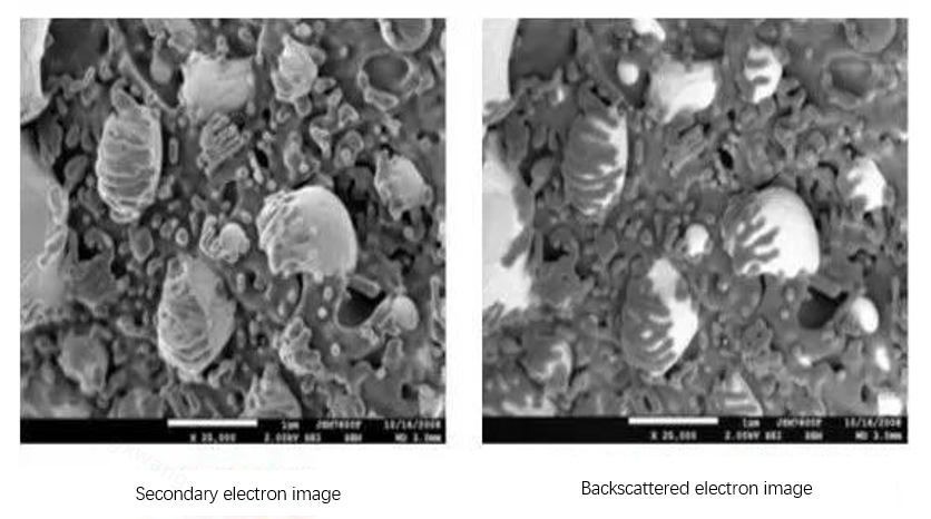
03 The key difference between secondary electrons and backscattered electrons.
In SEM analysis, secondary electrons and backscattered electrons are two of the most commonly used imaging signals, and they have many differences:
Generation mechanism: Secondary electrons are generated when incident electrons interact with electrons outside the nucleus, knocking out the outer electrons of the sample atoms. Backscattered electrons are high-energy electrons that bounce back after incident electrons undergo elastic or inelastic scattering with atomic nuclei.
Information depth: Secondary electrons come from the extremely shallow surface layer (5-10nm), while backscattered electrons come from deeper regions (several hundred nanometers).
Imaging characteristics: The secondary electron image is sensitive to surface morphology, with high resolution (up to 1nm for field emission electron microscopy), no obvious shadow effect, and strong three-dimensional image perception.
Backscattered electron images show composition contrast (atomic number contrast), with a relatively low resolution (usually 50-200nm), and the image is relatively flat
Application direction: Secondary electrons are mainly used to observe the microscopic morphology of the surface, such as fracture analysis, surface structure, etc. Backscattered electrons are used to distinguish different component regions, phase distribution analysis, etc.
Energy level: Low secondary electron energy (0-50eV); The energy of backscattered electrons is high (close to that of incident electrons, usually greater than 50eV).
04 The Application of SEM in PCB Manufacturing and Failure Analysis
SEM has extensive applications in the fields of PCB manufacturing and PCBA assembly, mainly reflected in the following aspects
Coating quality analysis(like finishing) is an important application of SEM in the PCB field. The electroplated copper inside the PCB board plays a role in signal transmission, and its crystal structure is directly related to the product quality.
By observing the crystal structure of electroplated copper through SEM, its ductility and tensile strength can be evaluated. High-quality electroplated copper has polygonal grains with a size of 2-6μm and no grain boundary defects. Poor-quality electroplated copper has a grain size of less than 1μm and poor ductility.
Alien substance contamination analysis is another important application of SEM. During the PCB manufacturing process, impure raw materials or process contamination can introduce impurities, leading to component failure.
By leveraging the morphology analysis capabilities of SEM and the elemental analysis capabilities of EDS, foreign substances can be quickly located and their components analyzed, which helps to trace pollution sources and improve processes.
For instance, in the analysis of foreign substances on the surface or in the holes, foreign substances containing Cl and Ag can be clearly detected by EDS. These residual chlorine residues can lead to a decline in the bonding force of the wire, causing it to fail.
Solder joint and interface analysis is of vital importance in the field of PCBA. SEM can be used to inspect the quality of solder joints and observe the continuity and uniformity of the interfacial reaction layer (IMC).
The absence of a continuous and uniform IMC layer can easily lead to poor bonding of solder joints. For the surface treatment of nickel plating gold, SEM can be used to observe the phenomenon of nickel corrosion, which is one of the typical reasons for poor tin absorption.
The evaluation of copper foil surface treatment is also a common application of SEM. Electrolytic copper foil needs to undergo surface treatment through electrochemical methods to generate microstructures and enhance adhesion to the substrate.
SEM can observe the Crystal grain structure produced by different additive formulations, guiding the optimization of process parameters. In the electroplating process, if the current density is too high, dendritic coatings will form brunch-like plated copper, causing copper powder to fall off and resulting in short circuits.
In the analysis of the inner black oxidation treatment for inner layer before lamination, SEM can be used to observe the microscopic morphology of the blackened(brown) copper surface. Blackening treatment can enhance the surface roughness of the inner copper foil, thereby strengthening the adhesion between the epoxy resin and the inner copper foil.
The microstructures formed by different black oxidation treatment methods (brown oxidation, black oxidation, and low-temperature blackening) each have their own characteristics. Choosing the appropriate process can prevent interlayer delamination after pressing.
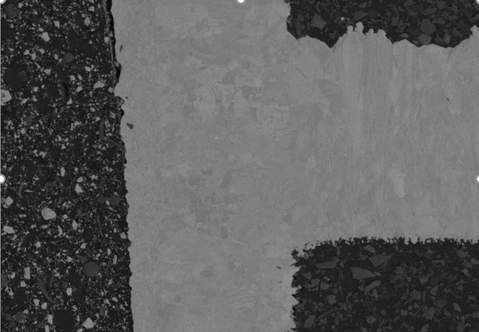
Cross-sectional analysis is an important means of PCB failure analysis. Many defects are difficult to observe on the surface. After obtaining a smooth cross-section through ion grinding or cutting, the SEM can be used to observe key information such as the crystallization state of the copper plating layer, whether there are voids or cracks between layers, and whether the IMC layer is continuous and uniform.
For instance, through cross-sectional analysis, it can be clearly observed that the nickel corrosion has penetrated into the copper layer.
Summary:
Applications of secondary electron images:
· Observe the roughness of the copper foil: evaluate its adhesion to the substrate.
· Inspect the appearance of the pads and circuits: Check for any scratches, depressions, burrs or other defects。
· Analyze the electroplating quality: Observe whether the crystallization condition of the electroplated copper is dense and uniform.
· Conduct cross-sectional analysis: Observe the quality of the hole wall after drilling, the resin contamination situation, and the bonding condition of the laminated interface.
· Observe the opening and coverage of the solder mask layer。
The application of backscattered electron images:
· Identification of foreign objects and contamination: If an unknown particle is found on the surface or in the hole of a PCB, it can be initially determined through the BSE image whether it is composed of heavy elements (such as solder sputtering, gold particles, etc.).
· Analyze the composition of the solder joints: Distinguish between solder (SnAgCu, high atomic number, bright) and copper pins (slightly lower atomic number, dark).
· Check the quality of the coating: for instance, observe whether the gold plating on the gold finger is uniform and if there is any exposed copper (copper is darker than gold).。
· Localization of IMC (intermetallic compounds) : In solder joints, the brightness of IMC such as Cu₆Sn₅ lies between that of solder and copper, which can assist in the initial localization.
In PCB manufacturing and failure analysis, secondary electron images are mainly used to observe the "appearance" (morphology), while backscattered electron images are mainly used to examine the "composition" (material). Typically, analysts will first use the SE mode to observe the overall morphology, identify the region of interest, then switch to the BSE mode to obtain component information, and finally use EDS for precise qualitative and quantitative elemental analysis. These three techniques complement each other and form the most powerful tool combination for PCB microscopic analysis.
Address:3-401, Dahong Technology Innovation Park, Xinyu Road, Shajing Street, Baoan District, Shenzhen
Q Q:172750477