


This is a very core and professional concept for PCB manufacturing to distinguish Panel Plating and Via filling Plating, it helps to understand its principle and make full use this knowledge in PCB Design and Manufacturing.
PCB Electroplating Process- The Principles and Differences between Panel Planting and Via-Filling Electroplating
This is a very core and professional concept for PCB manufacturing to distinguish Panel Plating and Via filling Plating, it helps to understand its principle and make full use this knowledge in PCB Design and Manufacturing.
One. Panel Plating
Principle
Panel electroplating, also known as "first time copper" or "thickened copper", is an electroplating step carried out after PCB drilling and before the transfer of circuit patterns.
The basic principle of electroplating copper shown below.
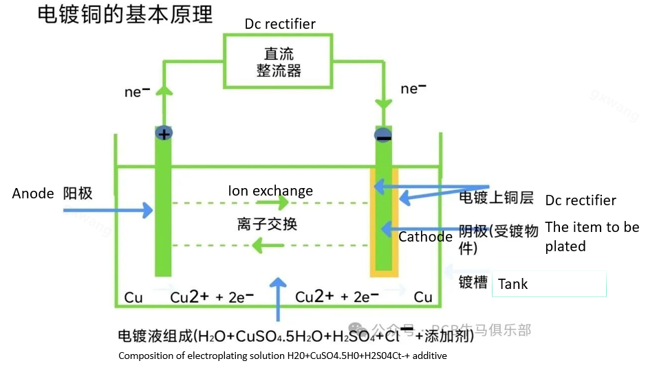
1. Pre-Process: Firstly, the already drilled copper clad laminate (CCL) is chemically cleaned to remove drilling dirt (resin residue) inside the holes and the oxide residue on the surface. Then, a very thin layer of Chemical copper (usually 0.3-0.5 microns) is deposited on the hole walls and inner copper rings through the Chemical Deposition process. The purpose of this layer of chemical copper is to make the originally non-conductive hole walls (glass fiber and resin) conductive, laying the foundation for the subsequent copper electroplating.
2. Electroplating process: The entire Panel is used as the cathode and immersed in an electroplating tank containing copper sulfate solution. After a direct current is applied, copper ions (Cu²⁺) in the solution move towards the cathode (plate) under the action of the electric field and are uniformly deposited and reduced to metallic copper on the chemical copper layer on the entire surface of the plate and the hole walls.
3. Purpose: The main purpose is to thicken the copper layer on the hole wall and surface to ensure that the copper thickness of the hole wall reaches a reliable level (usually above 5-8μm), so as to guarantee the electrical connection (conduction) and mechanical strength of the hole. Without this step, relying solely on the thin layer of chemical copper plating, the hole wall would be extremely fragile, prone to breakage during subsequent processing, and have poor electrical conductivity.
In simple terms, panel plating is to uniformly "coat" the entire board (including all through holes and blind holes) with a uniform copper outer layer, thereby enhancing its electrical conductivity.
Two. Via Filling Plating
Principle
· Via filling plating is a special electroplating process, mainly used for blind holes or through holes as well. Its purpose is not to thicken evenly, but to completely fill all the blind holes with copper.
The progress of Via filling Plating is shown below.
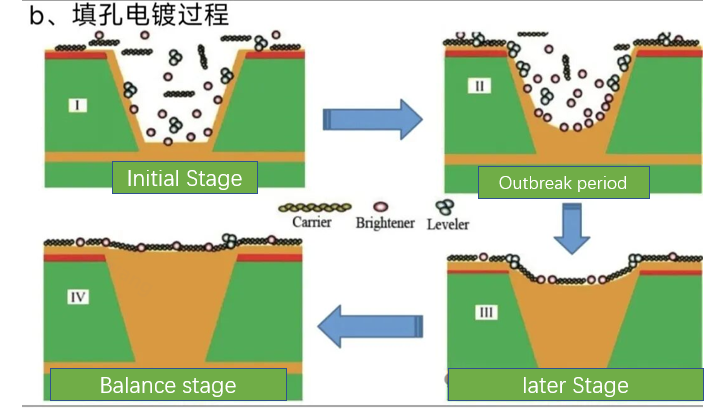
Principle of via filling plating
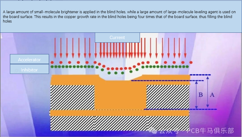
1. Special electroplating solutions and additives: Hole filling electroplating uses special electroplating solutions and high content of organic additives (inhibitors, accelerators, and leveling agents).
·
· Accelerator: Accelerates copper deposition in holes and micro-depressions.
·Inhibitor: Inhibits the deposition rate of copper in the flat area of the via surface and at the orifice.
· Leveling agent: Further optimize the filling effect and prevent the formation of voids.
2. Electroplating process: Under the influence of the electric field and additives, the deposition rate of copper in the holes is much faster than that on the plate surface. Electroplating starts to grow rapidly from the bottom and middle of the hole wall and eventually converges at the center of the hole, thus completely filling the entire blind hole with solid copper without excessive thickening of the surface copper layer.
3. Purpose:
· Preparing for subsequent lamination: After the holes are filled, another layer of circuit can be perfectly superimposed on them to achieve higher-density interconnections (HDI boards).
· Improving electrical performance: The thermal conductivity and electrical reliability of solid copper holes are better than those of ordinary electroplated holes.
· void problems such as resin plug holes: It provides a more reliable interconnection method.
In simple terms, hole-filling electroplating is like "3D printing", precisely filling the solid inside of a blind hole with copper while keeping the surface flat.
Three: Sum Up
Characters | Panel Plating | Via filling Plating |
Purpose | Evenly thicken the copper layer on the entire plate surface and hole walls Ensure the reliability of conduction. Short-term electroplating is also acceptable It is used as a flash plating base before filling holes | Completely fill the blind holes, providing for stacked holes and high-density wiring Flat surface. |
Process stage | After drilling, before the pattern is transferred | After drilling, before the pattern is transferred |
Processing object | The entire board (with all through holes, blind holes as the base and buried holes and the board surface) | Specific laser blind holes or mechanical blind via, considering through-hole copper or outside face copper |
Technical core | For conventional electroplating solutions, uniform deposition is pursued and a relatively good through-hole filling rate is achieved | Special electroplating solutions and additives are used to pursue differentiated deposition (fast in-hole and slow surface rise), resulting in a poor through-hole filling rate |
Differences in Chemicals | The content of copper sulfate in the high-acid and low-copper electroplating solution is 50-90g/L, and that of sulfuric acid is 110-130ml/L | The content of copper sulfate in the low-acid and high-copper electroplating solution is 220-260g/L, and that of sulfuric acid is 30-50n /L |
Result form | A uniform copper layer is formed on the hole wall of the through hole | Fill the blind holes completely with solid copper, ensuring a smooth surface. |
Main applications | Through-hole manufacturing for all types of PCBS (the most basic process) | Blind vias of HDI high-density interconnect boards (for mobile phones, high-end CPUs, etc.) |
Four、The relationships of these 2 process flow
A typical HDI board manufacturing process would involve both of these processes simultaneously:
1. Inner layer drilling -> Copper immersion ->" Full plate electroplating (negative film process, thickening all holes and surfaces)
2. Outer layer pattern transfer (dry film application, exposure, development)
3. Pattern plating (secondary copper in the positive film process, further thickening the circuits and pads)
4. For boards that require via filling plating plugged: During or after the graphic electroplating stage (positive film process), use the hole filling electroplating process to fill the specific blind holes.
5. Subsequently, processes such as film removal, etching, and film stripping are carried out (positive film).。
Conclusion
Full-board electroplating is a fundamental and universal step in PCB manufacturing, aiming to establish reliable metallized holes. Via-filling plating is a specialized and advanced technology for high-end HDI boards, aiming to achieve smaller and denser stack hole interconnections.
They are not an either-or choice, but two key electroplating technologies adopted at different manufacturing stages and for different purposes.
Special Note: The above discussion is for reference only and serves as a starting point for further discussion! The chemicals, processes, equipment, product structures and many other factors in each factory are all different. It is absolutely not advisable to copy them blindly or directly apply experience. All effective improvement measures come from experimental data! As one of the professional qualities of engineering and technical personnel, it must be "out of real practice."
Address:3-401, Dahong Technology Innovation Park, Xinyu Road, Shajing Street, Baoan District, Shenzhen
Q Q:172750477