


PCB back drilling process: A key manufacturing technology for enhancing high-speed signal integrity
Back drilling process in PCB manufacturing: What are the basic principles and purposes? Is it different from traditional through-hole drilling?
PCB back drilling process: A key manufacturing technology for enhancing high-speed signal integrity
In the fields of high-speed digital circuits and RF microwave, the PCB back drilling process can significantly enhance signal integrity by removing redundant via stubs, and it is an indispensable key technology in modern electronic manufacturing.
In modern electronic devices, especially in the fields of high-speed digital circuits and radio frequency microwave, the signal integrity of printed circuit boards (PCBS) is of vital importance. Back Drilling, as a specialized PCB manufacturing process, significantly enhances high-frequency performance by removing unused conductive parts from vias.
This article will provide a detailed analysis of the definition, principle, application scenarios, specific process and key control points of the back drilling technology
1.What is the back drilling process?
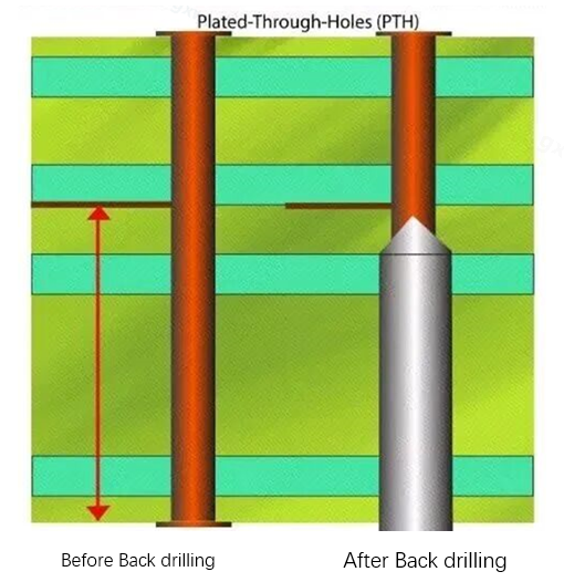
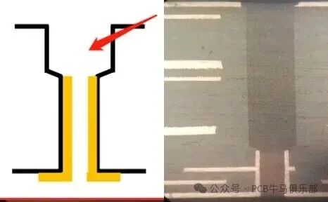
。Back drilling, also known as depth control drilling or back drilling, is a PCB manufacturing process that removes the excess copper tubes (referred to as "stubs" or "stub") that are not connected or transmit signals in the through holes of multi-layer boards through secondary drilling.
When a multilayer board needs to transmit signals from the first layer to the ninth layer, traditional through-holes cause the hole walls to be entirely copper-plated for conduction from the first layer to the bottom layer. In fact, only the connection from layer 1 to layer 9 is needed, and the part from layer 10 to the bottom layer becomes redundant stubs.
这个stub在高频信号传输中会像天线一样产生辐射,引起信号反射、散射和延迟,导致信号完整性下降。背钻工艺就是从PCB的背面(或正面)进行二次钻孔,精确去除这部分多余的stub。This stub will generate radiation like an antenna during high-frequency signal transmission, causing signal reflection, scattering and delay, resulting in a decline in signal integrity. The back drilling process involves performing secondary drilling from the Top (or bottom) of a PCB to precisely remove the excess stubs in this area.
2. The working principle of a back drill
背钻工艺的核心原理是利用直径稍大于原始过孔的钻头,从板的一面进行控深钻孔,精确去除多余的铜筒部分,同时保留所需部分的电气连接。The core principle of the back drilling process is to use a drill bit with a diameter slightly larger than the original through hole to perform controlled depth drilling from one side of the plate, precisely removing the excess copper cylinder part while retaining the electrical connection of the required part.
Fundamentals of Technology:
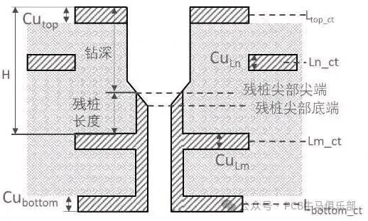
· The size relationship of the drill bit: The diameter of the back drill bit is usually 8-10mil (0.2-0.25mm) larger than that of the original through-hole to ensure the complete removal of the target stub without damaging the surrounding structure.
· Depth control: The depth of the back drill needs to be precisely controlled to stop above the target signal layer without damaging it. It is generally required that the remaining stub length be controlled within the range of 50 to 150μm.
Depth computing:
The depth of the back drill can be calculated by the formula: Back drill depth = (Total PCB thickness - thickness from the end layer to the bottom of the board) ± process compensation value.
For instance, if the total thickness of a PCB is 1.6mm and the stubs below L5 in the holes from the surface layer (L1) to L5 need to be removed, the back drilling depth should be "the thickness from L1 to L5 + 0.05mm compensation" (to avoid damaging L5).
3. The application scenarios of back drilling technology
Back drilling technology is mainly applied in high-speed circuit fields with high requirements for signal integrity:
· Communication equipment: 5G base stations, routers, switches, etc., are used to improve the quality of high-speed data transmission.
·High-performance computing: large servers, supercomputer motherboards.
· Advanced medical electronics: Medical imaging equipment, diagnostic instruments.
· Aerospace and military: Radar systems, aerospace electronic equipment
The application of back drilling needs to take cost factors into account, as it will increase the PCB manufacturing cost by approximately 20-30%, but it is one of the most cost-effective solutions in high-speed (typically 5Gbps) signal scenarios.
4. The specific process of back drilling technology
The back drilling process mainly consists of the following steps:
1. One-time drilling: Use positioning holes to position the PCB and perform the first drilling (through holes).
2.Pre-treatment before electroplating: Dry film sealing treatment is carried out on the positioning holes to prevent the electroplating solution from entering.
3. Electroplating: Electroplating is applied to the PCB after one drilling to metallize the hole walls.
4. 外层图形制作:在电镀后的PCB上制作外层电路图形。
5. 图形电镀:在进行图形电镀前,再次对定位孔进行干膜封孔处理。
6. 背钻定位:利用一次钻孔使用的定位孔进行背钻定位。
7. 背钻:采用控深钻技术对需要背钻的电镀孔进行二次钻孔。
8. 清洗:背钻后对背钻孔进行水洗,清除孔内残留的钻屑。
4. Outer layer pattern creation: Create the outer layer circuit pattern on the PCB after electroplating. 5. Pattern plating: Before performing pattern electroplating, dry film sealing treatment should be carried out on the positioning holes again.
6. Back drilling positioning: Use the positioning holes used in one drilling session for back drilling positioning.
7. Back drilling: Use depth-controlled drilling technology to conduct secondary drilling on the electroplated holes that require back drilling.
8. Cleaning rinse: After back drilling, wash the back hole with water to remove any remaining drill residue inside the hole.
This process ensures the accuracy of back drilling and avoids quality problems caused by multiple processing.
5. Key points for controlling the back drilling process
The successful implementation of the back drilling process requires strict control of the following key points:
5.1 Depth accuracy control
背钻深度控制是工艺核心,要求偏差通常控制在±0.05mm以内,高频板甚至需要±0.025mm的高精度。
控制措施包括:
· 高精度设备:使用Z轴定位精度≤±0.01mm的高精度钻机,配备光栅尺或激光位移传感器实时监测钻尖位置。
· 钻头长度校准:新钻头或更换钻头后,使用钻头长度测量仪(精度±0.001mm)测量实际长度,并录入系统补偿。
· 板厚测量:多点测量PCB实际厚度,根据实测值修正背钻深度。
5.2 Positioning accuracy control
背钻与原始孔位的对准精度至关重要,偏差过大会损伤内层线路。
改进方法包括:
· 采用专门的定位孔处理技术,防止因电镀导致的尺寸变化。
· 使用CCD光学对位系统,识别板边Mark点,补偿PCB涨缩。
5.3 Drill bit selection and wearing management
· 钻头尺寸:背钻头直径比原始孔大0.2mm左右(约8-10mil)。
· 磨损补偿:钻尖磨损会导致有效切削深度减少,需通过计数补偿或图像识别检测钻尖磨损量。
5.4 The materials are compatible with the design
· 介质厚度:背钻停止层到下一层的介质厚度应≥0.17mm。
· 间距要求:背钻孔距内层图形≥0.25mm,距外层图形≥0.3mm。
· 表面处理:背钻PCB表面处理宜采用OSP或化学沉锡,禁用HASL(热风整平)
6. Quality inspection of back drilling process
背钻后的质量验证同样重要,主要检测方法包括:
· 切片分析:金相切片测量stub残留长度和背钻底部到内层的距离。
· X-Ray检测:通过X射线透视观察孔底是否与目标内层对齐。
· 阻抗测试:测量背钻后的阻抗值,间接验证stub残留是否达标。
Summary
背钻工艺通过去除高速PCB中过孔的多余stub,能显著提升信号完整性,减少反射和干扰。随着5G、高速计算和人工智能技术的快速发展,对背钻工艺的需求将持续增长。
掌握背钻技术的原理、流程和控制要点,对于设计和生产高性能电子设备具有重要意义。随着材料科学和精密加工技术的进步,背钻工艺的精度和效率将进一步提高,为未来高速电子设备的发展提供坚实支撑。
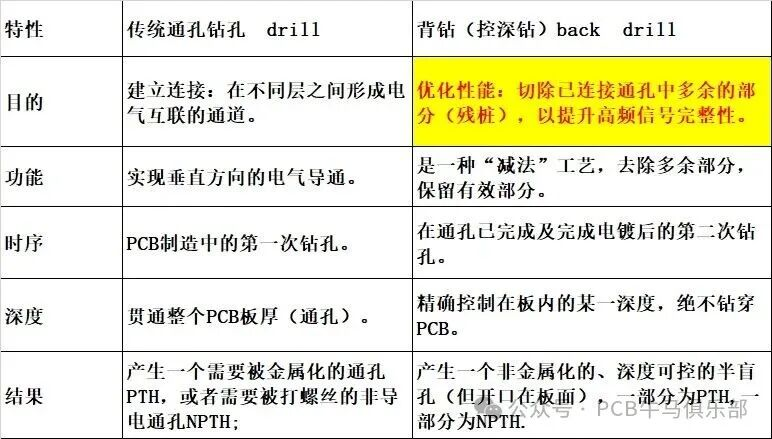
背钻的本质:与传统的钻孔来进行对比,本质上就是控深钻孔。背钻(控深钻)VS 传统钻孔:本质区别与实现原理详解
1、Essential difference: Purpose and function
To understand the difference between the two, one must first realize that their purposes are completely different.
 ·
·
Core metaphor:
· 传统钻孔:像在盖房子时浇筑一根从楼顶贯通到地下室的水管,目的是让水能从上流到下。
· 背钻:像房子盖好后,发现地下室那段水管用不到反而会产生回音,于是从地下室精确地向上钻一段,切掉那段多余的水管,同时绝不能损坏楼上还在使用的水管。
2、Implementation principle: How to precisely control depth?
背钻工艺的实现,核心在于 “深度控制” 。这并非通过简单的机械限位来实现,而是一套集高精度机械、传感技术、软件补偿和材料学于一体的精密系统。其工作原理和流程如下图所示:
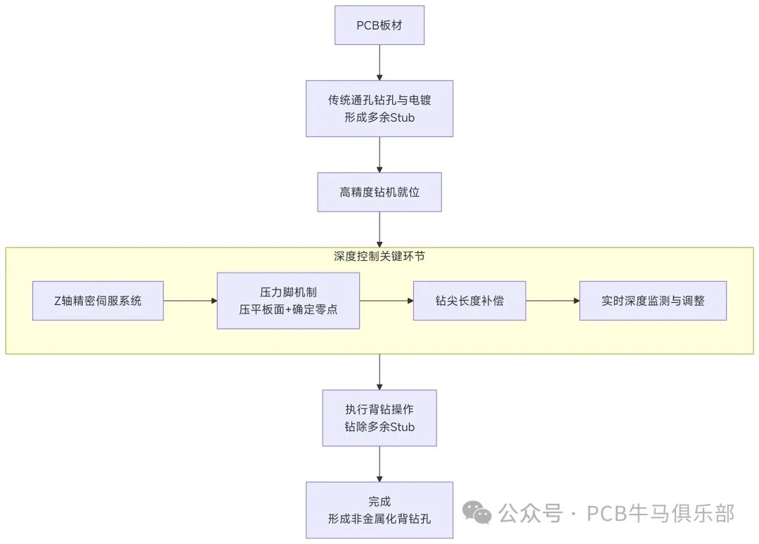
A. 高精度机械平台 (Z轴精密伺服系统)
背钻设备的核心是拥有极高定位精度和重复精度的Z轴伺服控制系统。该系统由伺服电机、高精度滚珠丝杠和光栅尺(一种高精度线性传感器)构成。
· 光栅尺:直接测量钻头滑台的实际位置,避免了丝杠热伸长、背隙等误差,将Z轴定位精度控制在±0.01mm以内。
B. 深度设定的基准——“零点”的确定
背钻深度不是从钻头尖开始算,而是从PCB板表面开始计算。如何确定“板面”这个零点至关重要。主要方法有:
· 机械接触传感:钻机使用一个叫“压力脚”的装置。先移动到目标孔位,压力脚下降并接触板面,传感器检测到接触压力后,系统即将此位置记录为Z轴零点。
· 激光定位:更先进的设备使用激光束测定板面高度,非接触式,速度更快。
C. 钻尖长度补偿 (Drill Tip Compensation)
这是深度控制中最容易被忽视但极其关键的一步。钻头不是平底的,而是有尖锐的刃角(通常为130°或140°)。当我们说“钻深5.0mm”时,是指钻头尖端进入板内5.0mm,但钻头肩部(实际切除铜皮的部分)进入的深度更浅。
· 补偿计算:控制系统会根据钻头的刃角、直径和板料类型,自动计算出一个补偿值。实际的进给距离 = 设定深度 + 补偿值。
· 示例:设定背钻深度为1.0mm,钻尖补偿值为0.1mm,则Z轴实际会进给1.1mm,以确保钻头肩部准确切除1.0mm深度处的铜层。
D. 工艺流程与深度控制
深度在制造过程中是通过一系列精细步骤保证的:
1. CAM编程:工程师根据叠层结构,精确计算出每批板、每种孔的目标背钻深度(Depth = 板总厚 - (目标层到参考层的距离 + 补偿值)),并输入NC钻床程序。
2. 板厚测量:对每块PCB进行多点测厚,取平均值输入钻机,钻机会根据实际板厚自动微调钻孔深度,抵消因板厚公差带来的误差。
3. 钻头管理:使用钻头长度测量仪精确测量每一支钻头的实际长度,并录入钻机系统,确保Z轴行程控制的准确性。
4. 实时监测与调整:高端钻机在钻孔过程中能通过监测主轴电流的变化,间接判断是否钻穿铜层(切削铜和切削基材的阻力不同),实现实时反馈和微调。
Three、深度控制的目标与挑战
· 目标:精准地将残桩(stub)切除,同时绝对不能损伤或钻到需要保留的那部分有效孔壁。
· 理想状态:背钻底部与需要保留的信号层孔壁之间留有75μm - 150μm的安全距离。
· 挑战:
· 过钻 (Over Drill):钻得太深,伤及有效孔壁,可能导致信号层连接中断或阻抗不连续。
· 欠钻 (Under Drill):钻得不够深,残留stub过长,未能完全达到改善信号完整性的目的。
· 对位偏差:背钻孔与原始孔中心偏离,可能导致钻到旁边的内层线路或保证不了stub被完全去除。
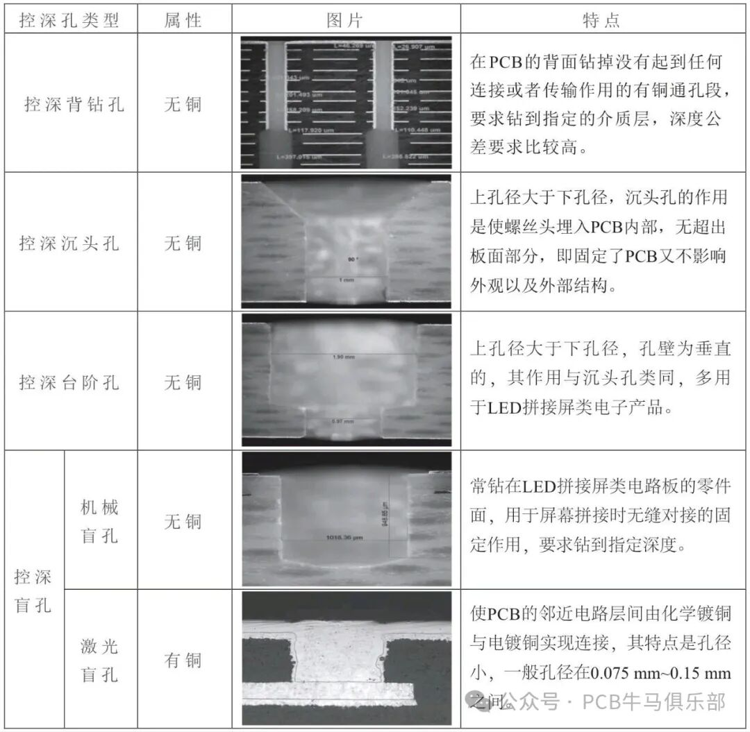
特别注意:有的工厂,利用机械钻刀钻出的控深盲孔,也被称为“背钻孔”,根据功能需要,可以做成PTH的(与激光盲孔功能一样),也可以是NPTH的,这类盲孔一般孔径比较大,直径在0.3mm_3.0mm之间,与激光盲孔的孔径有明显的区别,激光盲孔的孔径一般在0.075mm_0.3mm之间。
General Summary
背钻与传统钻孔的本质区别在于其“二次、控深、减法” 的特性。其实现原理远非“钻得浅一点”那么简单,而是依托于:
1. 高精度机电系统(光栅尺、伺服电机)提供基础精度。
2. 精密的传感与定位(压力脚、激光)确定基准零点。
3. 复杂的软件算法(钻尖长度补偿、板厚补偿)进行实时计算和调整。
4. 严格的流程管理(钻头测量、CAM编程)确保过程受控。
特别说明:以上的探讨仅供参考,起到抛砖引玉的作用!每个工厂的药水/工艺/设备/产品结构等等,多种因素都有差异性,千万不能生搬硬套,万万不能将经验直接拿来使用,一切有效的改善措施,都来源于试验数据!作为工程技术人员的职业素养之一,一定是“拿数据说话。
Address:3-401, Dahong Technology Innovation Park, Xinyu Road, Shajing Street, Baoan District, Shenzhen
Q Q:172750477